Lab Five: RF Amplifier
One of the final components needed for this AM radio is to add an RF amplifier. The RF amplifier will take in the signal from the antenna constructed in Lab 6, and amplify it to be fed into the AM detector. This RF amplifier includes an inductor that allows DC currents to pass through and High Frequency AM signals to be amplified.
RF Amplifier Construction
The Common Source amplifier shown in Figure 1 is created on the breadboard as shown in Figure 2. This amplifier utilizes a JFET chip rather than a BJT. A JFET chip has similar characteristics of a BJT chip, but offers a very high input resistance making it ideal for a cascaded stage of a multi-stage amplifier. In the final design, this will be stage two of the RF amplifier.
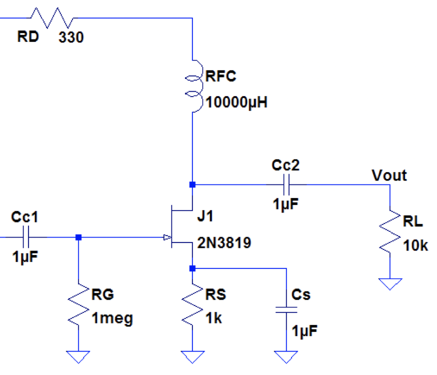
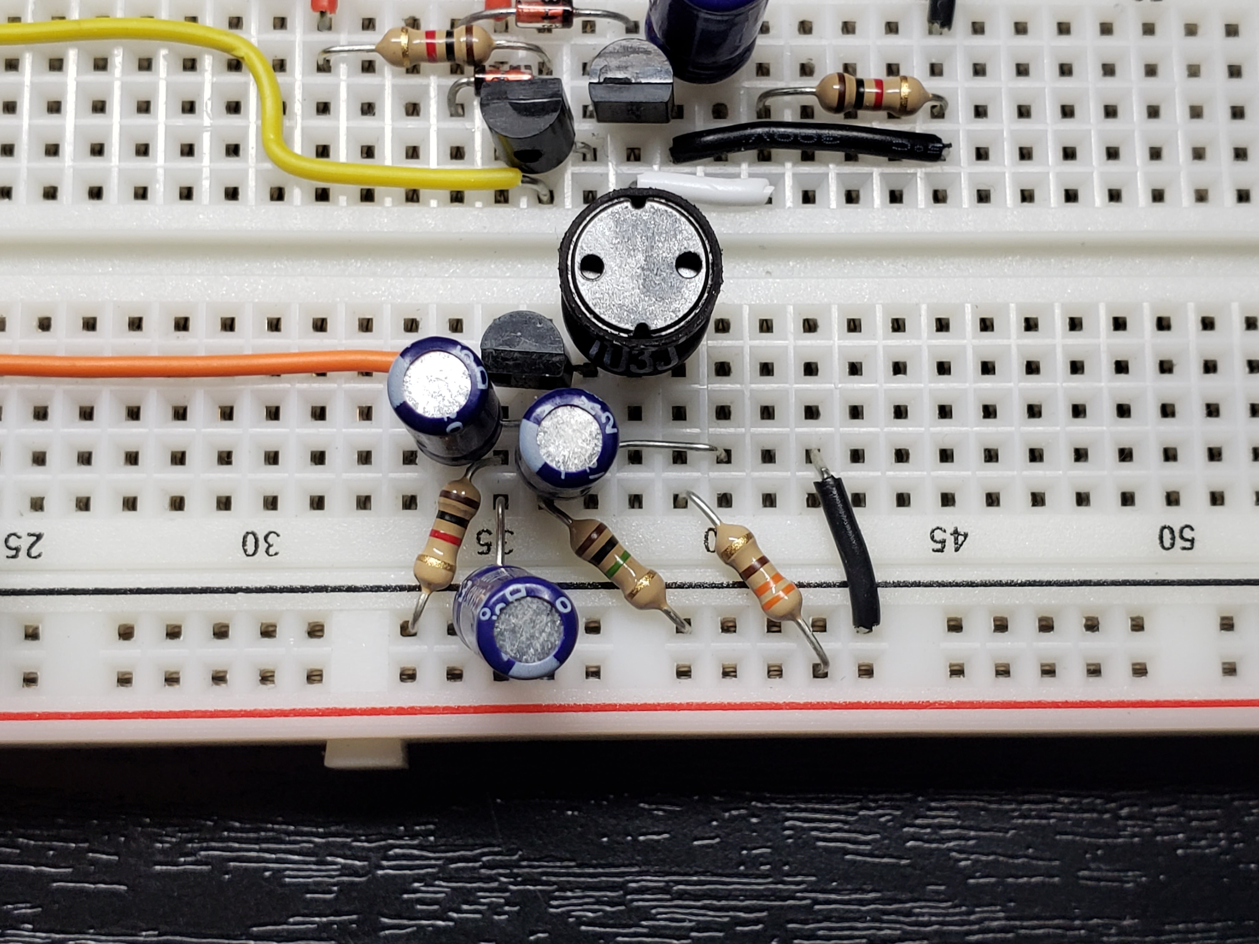
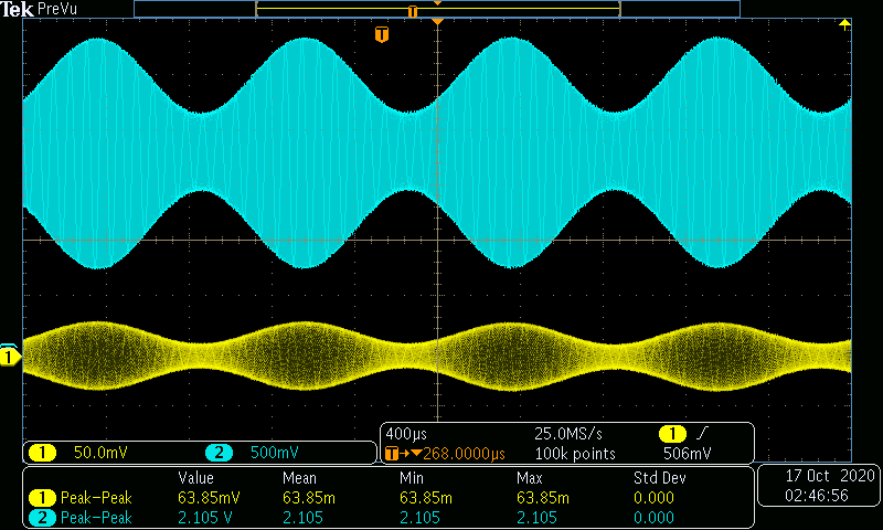
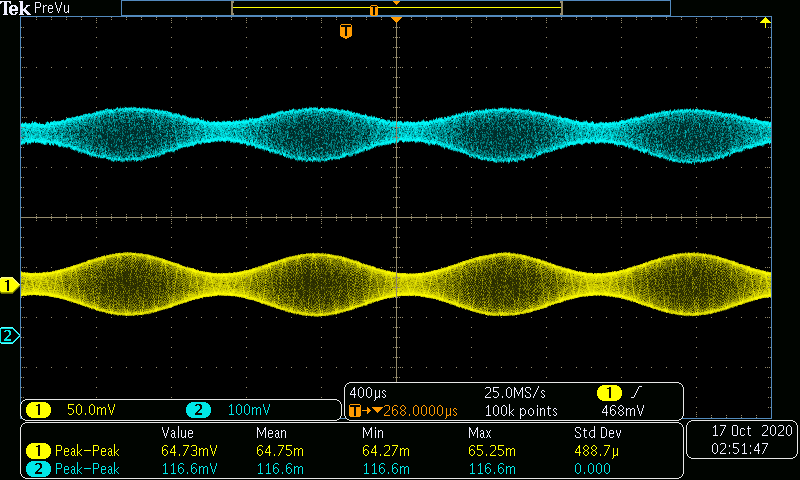
Using the circuit pictured above in Figure 1 and 2 the following data in Table 1 is collected by changing the value of \(R_L\). Table 1 is further filled out by adding in an RF Choke (RFC) inductor to the drain of the FET. This created a high impedance for high frequency signals and a low impedance for lower frequencies. Because this stage comes before the AM detector, the signal that we want to be amplified is of high frequencies. This high impedance ensures that a clear signal is amplified. Figure 3 shows an \(R_L\) value of \(10k\Omega\) without the RFC and Figure 4 shows an \(R_L\) value of \(1k\Omega\) with the RFC.
\begin{array} {|c|c|c|c|} \hline & R_L=1M\Omega& R_L=10k\Omega & R_L=1k\Omega\\ \hline Q(V_{DS},I_D) & (8.24V, 545\mu A) & (8.19V, 757\mu A) & (8.12, 878\mu A)\\ G(\frac{V}{V})~No~RFC & 2.74 & 2.28 & 1.81 \\ G(\frac{V}{V})~With~RFC & 54.3 & 33.41 & 6.0 \\ \hline \end{array}
Next, the common emitter amplifier of Figure 5 is created as shown in Figure 6. The Q piont for the npn BJT is measured to be \((1.68V, 11mA)\). The BJT common emitter amplifier output is fed into the gate input of the JFET common sourse amplifier through a bypass capacitor.
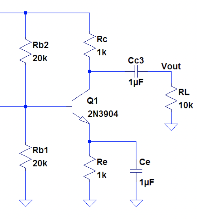
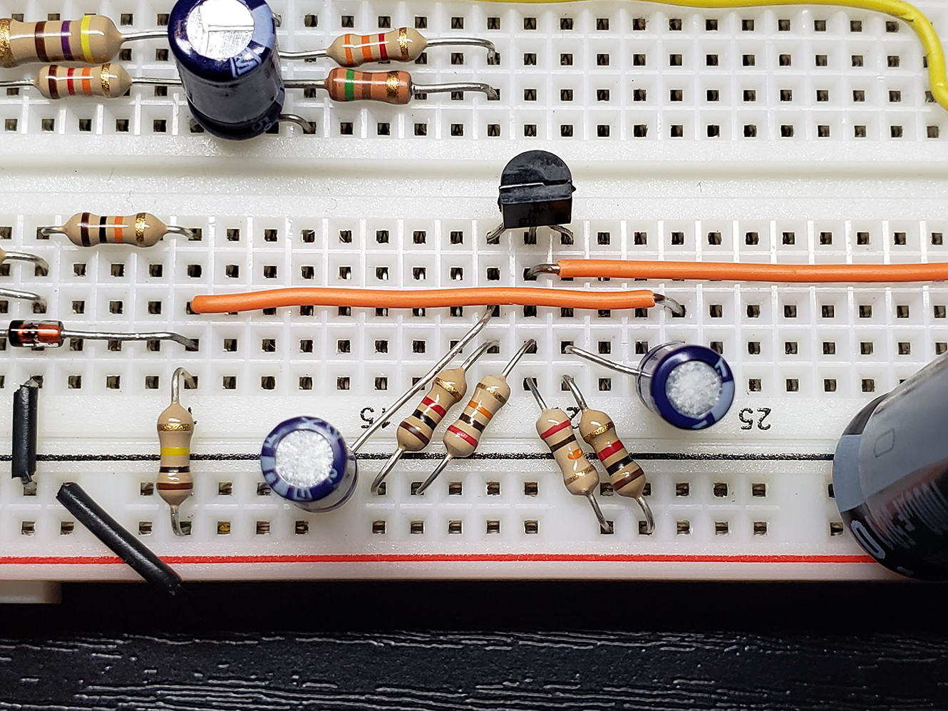
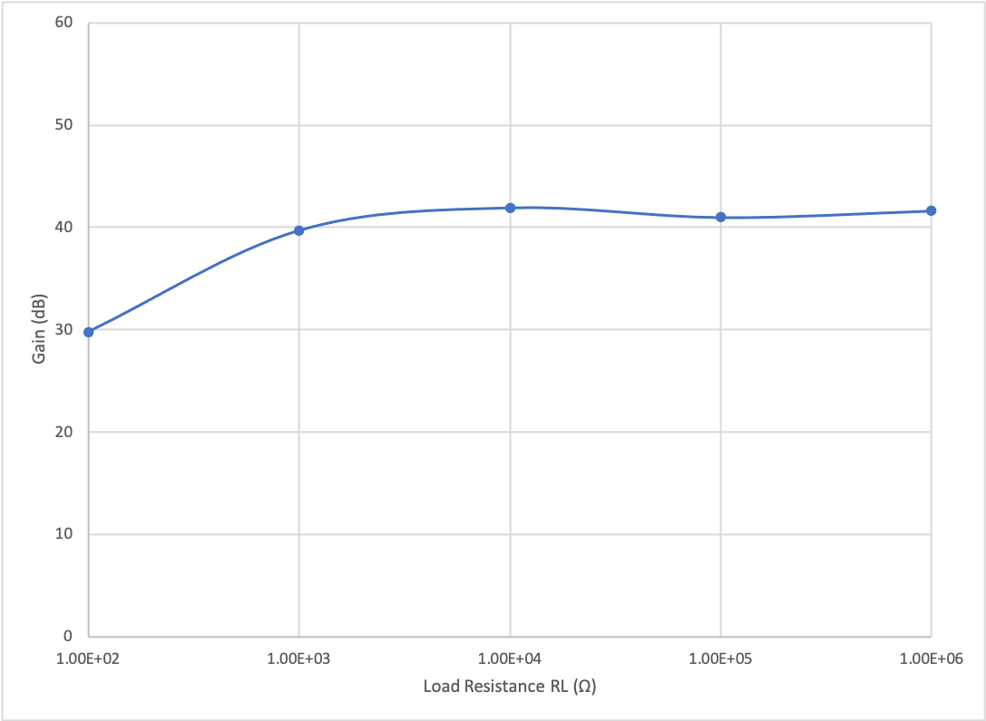
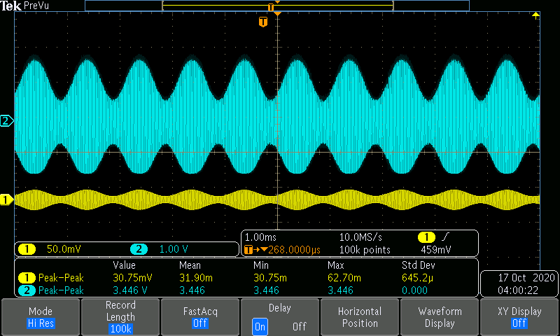
Table 2 shows different gain values for several values of \(R_L\) ranging from \(1M\Omega-100\Omega\). A plot of this table can be found in Figure 7. This data shows that when combining the two amplifiers, it can be expected to have a high gain value. \(R_L\) in this case will the the AM Detector with the audio amplifier connected. The audio amp was designed to have a very high input impedance, so it will combine nicely with the RF amplifier. Figure 8 shows an \(R_L\) value of \(1M\Omega\) and its corresponding input and output waveforms.
\begin{array} {|c|c|c|} \hline R_L & Gain(\frac{V}{V}) & Gain(dB)\\ \hline 1M\Omega & 120.625 & 41.62\\ 100k\Omega & 112.06 & 40.98\\ 10k\Omega & 125.03 & 41.94\\ 1k\Omega & 96.875 & 39.72\\ 100\Omega & 31.54 & 29.79\\ \hline \end{array}
Conclusion
The only next step left is to connect the RF amp to the AM detector and connect the AM detector to the multi-stage audio amp. Upon completing this, when touching the large 1000µF capacitor an audible sound is able to be heard through the speaker. This is largely due to the waves that my body is able to pick up and is then fed through the ground connection into the RF amplifier. This lab brings many different concepts together into creting a functional AM radio and the processing of analog and RF circuits.